Nano-electronics
Since the discovery of graphene via mechanical exfoliation, it has been shown that the electronic properties of solids can undergo dramatic change when the material thickness is reduced to the atomic limit. Notably, even the band structures of single-layers and bi-layers can be distinctively different in both graphene and transition metal dichalcogenides (TMDs). Their exotic bandstructures are uniquely different from those in conventional 2DEGs. In particular, the broken inversion symmetry and strong spin-orbit interaction in semiconducting TMDs polarize spins in the opposite direction near the band edges of each valley. This combined valley-spin degree of freedom provides new platforms for exotic emergent quantum phenomena and possible quantum device application. With the help of electron-beam-defined local depletion gates, the system dimension can be further reduced to be mesoscopic, where relevant device dimensions become comparable to the electron wavelength. In such gate-defined nanostructures, gate-tunable quantization can be achieved while preserving and manipulating the quantum phase coherently.
Quantum Confinement in TMD
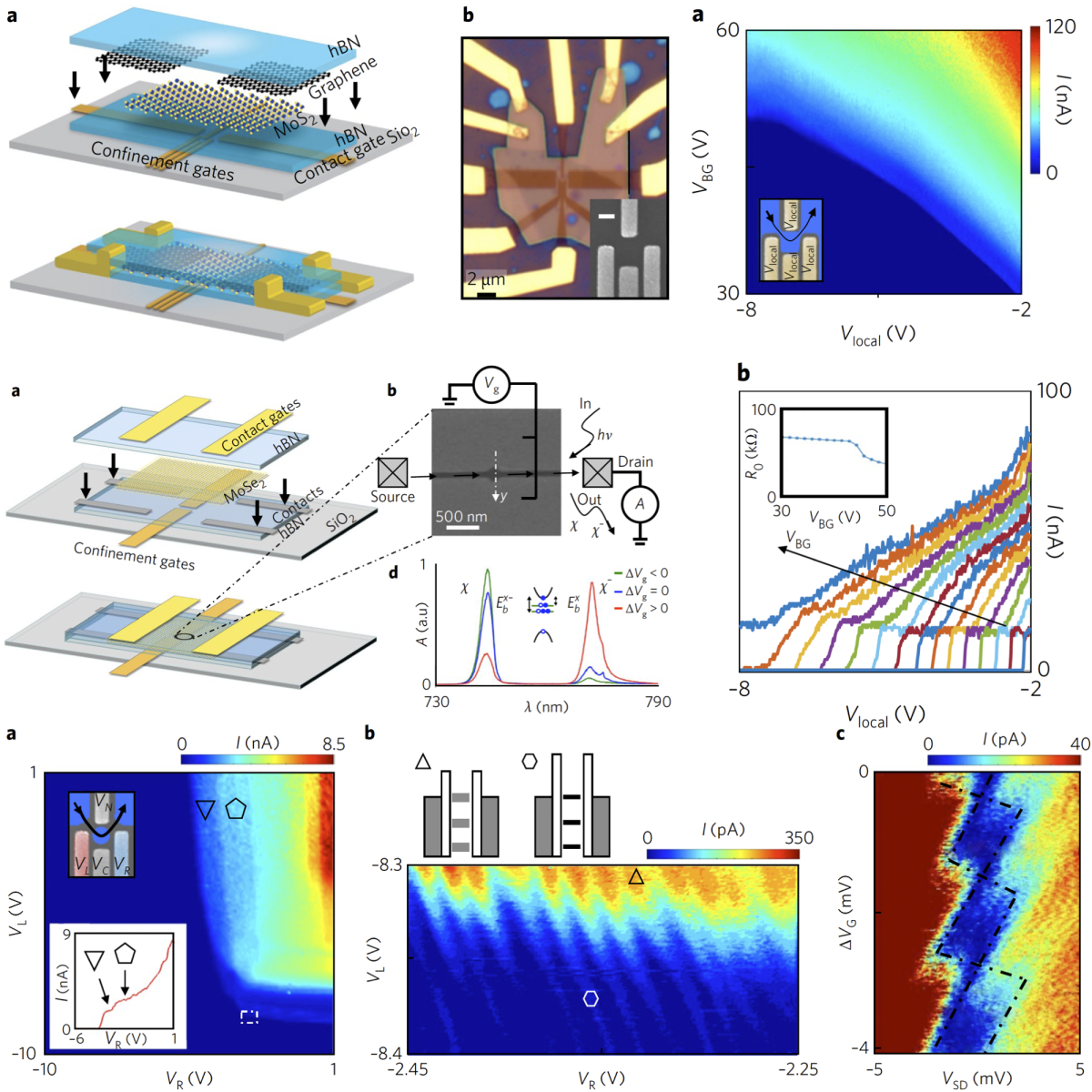
Electrical confinement and manipulation of charge carriers in semiconducting nanostructures are essential for realizing functional quantum electronic devices. The unique band structure of atomically thin transition metal dichalcogenides (TMDs) offers a new route towards realizing novel 2D quantum electronic devices, such as valleytronic devices and valley–spin qubits. 2D TMDs also provide a platform for novel quantum optoelectronic devices due to their large exciton binding energy. However, controlled confinement and manipulation of electronic and excitonic excitations in TMD nanostructures have been technically challenging due to the prevailing disorder in the material, preventing accurate experimental control of local confinement and tunnel couplings. Here we demonstrate a novel method for creating high-quality heterostructures composed of atomically thin materials that allows for efficient electrical control of excitations. Specifically, we demonstrate quantum transport in the gate-defined, quantum-confined region, observing spin–valley locked quantized conductance in quantum point contacts. We also realize gate-controlled Coulomb blockade associated with confinement of electrons and demonstrate electrical control over charged excitons with tunable local confinement potentials and tunnel couplings. Our work provides a basis for novel quantum optoelectronic devices based on manipulation of charged carriers and excitons.
Electrical Control of Charged Carriers and Excitons in Atomically Thin Materials
K. Wang, K. D. Greve, L. A. Jauregui, A. Sushko, A. High, Y. Zhou, G. Scuri, T. Taniguchi, K. Watanabe, M. D. Lukin, H. Park, P. Kim
Nature Nanotechnology 13, 128–132 (2018)
Imaging electron flow and quantum dot formation in MoS2 nanostructures
S. Bhandari, K. Wang, K. Watanabe, T. Taniguchi, P. Kim, R. M. Westervelt
Nanotechnology (2018)
Magnetotransport Studies of Mobility Limiting Mechanisms in Undoped Si/SiGe Heterostructures
X. Mi, T. M. Hazard, X. Mi, K. Wang, J. R. Petta
Phys. Rev. B 92 (3), 035304 (2015)
A Reconfigurable Gate Architecture for Si/SiGe Quantum Dots
D. M. Zajac, T. M. Hazard, X. Mi, K. Wang, J. R. Petta
Appl. Phys. Lett. 106, 223507 (2015)
Charge Relaxation in a Single-electron Si/SiGe Double Quantum Dot
K. Wang, C. Payette, Y. Dovzhenko, P. W. Deelman J. R. Petta
Phys. Rev. Lett. 111, 046801 (2013)
Electrically controlling single spin coherence in semiconductor nanostructures
Y. Dovzhenko, K. Wang, M. D. Schroer, J. R. Petta
Book chapter in "Quantum Dots: optics, electron transport and future applications", edited by A. Tartakovskii, Cambridge University Press (2012)
C. Payette, K. Wang, P. J. Koppinen, Y. Dovzhenko, J. C. Sturm, J. R. Petta
Appl. Phys. Lett. 100, 043508 (2012)