Photolithography Laboratory: Patterning a Wafer
Objective
Photolithography is the most critical process step in device fabrication. The main goal of photolithography is to replicate a pattern representing an integrated circuit component on the wafer surface.
In this lab you will simulate the four key stages of photolithography that are typically carried out in an IC fabrication:
- Surface preparation
- Application and exposure of photoresist
- Development or removal of specific areas of photoresist
- Inspection
You will conduct a study how exposure and development processes affect the quality of the pattern replication.
Consumable Materials
- Gloves (light duty latex or equivalent)
- 4” silicon wafers, pre-cleaned
- Isopropyl alcohol (rubbing alcohol is acceptable)
- Deionized water
- Can of compressed air (or a source of clean, dry, particle free compressed air)
- Photoresist (needs to be in a dark-colored plastic bottle)
- Developer solution (1:5 solution in DI water), compatible with photoresist ● Clean room wipes or other lint-free laboratory wipes
- Disposable plastic droppers
Equipment
- A hotplate with a temperature readout, preset to 105ºC
- Spin coater
- Containment box (plastic, about 18 x12 x 9 l x w x d)
- Safety glasses/goggles
- Tweezers
- Digital timer
- Solvent waste container and funnel
- One 500mL beaker for mixing developer solution
- Developer tray (shallow, wide enough to immerse wafer)
- Transparent mask with pattern to be transferred
- Desk lamp with a compact fluorescent bulb (at least 15W recommended)
- Note: LED or tungsten lamps will not work
Photolithography Lab Procedure
- Cleaning and drying the wafer
To apply a good layer of photoresist, it is essential that the substrate be free of oils, dirt, or previous photoresist layers. In a semiconductor fab, wafers are cleaned by immersing them in a series of solvents. In this lab, you will use pre-cleaned wafers, which need only light finish cleaning and drying of the wafer surface.- Place two pre-cleaned wafers on a dry, clean wipe.
- Squirt a small quantity of isopropanol on each wafer and gently wipe with a clean room wipe. Allow the alcohol to dry from the wafers.
- Blow-dry the front of the wafers with particle-free compressed air.
- Place the wafers on the hotplate set at 150°C for 60 seconds to drive off any remaining water. Allow to cool.
- Applying Photoresist
The photoresist should be applied in a thin, uniform layer to ensure success in the subsequent etching step. Here we use a simple spin coater to spread the photoresist in a layer approximately 20-50 microns thick.- Place the spinner inside the containment box. Line the box with paper towels to catch excess photoresist.
- Place a wafer on the spinning device so that the flat of the wafer is next to a peg on the spinner disk. Rotate the wafer about 20 degrees so that the outer edge is under all three pegs.
- Position the spinner so that its center is directly under the hole in the lid of the containment box. Place the lid on the box to check alignment, and adjust if needed.
- With the lid on, turn the spinner on and allow it to run about 30 seconds to reach full speed.
- While the spinner is spinning up to speed, open the bottle of photoresist. Withdraw enough photoresist into a disposable dropper to fill about 2-3 cm up from the bottom of the dropper tip.
- When the spinner has reached full speed, insert the dropper into the hole in the box lid. Try to position the dropper directly over the center of the spinning wafer.
- Squirt all the photoresist in the dropper onto the wafer in one continuous motion (i.e., don’t stop and start but apply all the dropper contents at once for a more even coating).
- Allow the spinner to run 30 seconds, then shut it off and allow the spinner to spin down.
- Repeat the process with your second wafer.
- Baking
The photoresist needs to be heated in order to optimize its photoreactive properties and to drive off solvents.- Place the wafers on the hotplate set at 80°C for 60 seconds.
- Allow the wafers to cool for 1-2 minutes. Keep the wafers out of direct sunlight and strong room light during this time.
- Exposure
In this step, the pattern on the mask is transferred to the wafer by interaction of light with the photoresist. At the end of this step, the image is virtual, that is, not visible until developed.- Place one wafer on a non-reflective surface.
- Place the photomask directly on the wafer. If using a chrome-on-glass mask, ensure that the correct side of the mask is down. This means that the side on which the pattern is printed should be in the down position, closest to the wafer.
- Position the compact fluorescent bulb about 12 cm above the mask. d. Expose the wafer for two minutes.
- Repeat this process for your second wafer, this time using a longer exposure period (three minutes).
- Development of Photoresist
Converting the latent image to a usable pattern requires chemical development to dissolve away the material that has been exposed to light. The developer in this case is a dilute solution of sodium hydroxide.- Submerge each wafer in the developer solution and agitate for 30 seconds. The pattern should gradually become visible.
- Remove the wafers from the developer bath and submerge then in the deionized water bath for two minutes.
- Remove the wafers from the water bath. Blow-dry the wafers using compressed air.
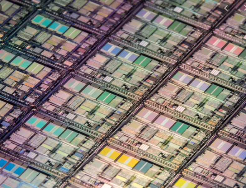
- Inspection
To determine the quality of the pattern transfer, examine the pattern you’ve made under a microscope at 40 to 100x.- Using the optical microscope, inspect the two wafers for:
- Underexposure: the pattern is incompletely transferred
- Overexposure: the pattern is “burned”, i.e., features are wider than they should be
- Overdeveloped: Too much of the photoresist has been removed from the edges of features
- Underdeveloped: photoresist remains in the areas where it should have been removed.
- Collect an image of the series of fine lines from each wafer. Record how well each of the lines was transferred to the developed pattern. Determine the smallest line on the image that has clean edges, free of irregularities. This is the lower limit of your pattern transfer accuracy. (Check with your instructor for details on what measures of resolution to use.)
- Using the optical microscope, inspect the two wafers for:
- Exercises
- With the results from the first two wafers, you have two data points that link two values of exposure time with two values of measured resolution. With your instructor, determine whether the wafer is over- or under exposed or over/under developed.
- Attempt to improve the pattern transfer by repeating the process with two other exposure times.
- First, remove the photoresist by a solvent cleaning procedure (immerse first in acetone, then methanol, then isopropanol, then water).
- Then, using the same light source at the same exposure distance, adjust the exposure or development times as follows. If your wafer was:
- overexposed: decrease light exposure by 30 seconds
- underexposed: increase exposure by 30 seconds
- overdeveloped: cut development time to 20 seconds
- underdeveloped: increase development time to 40 seconds or more
- Repeat steps 2-6 of the procedure above.
- Inspect the new pattern on each of your wafers, as in step 6 above.
- Collect images and obtain data on the lower resolution limit of the second set of wafers.
- Clean and dry your wafer and return to your instructor.
8. Analysis and Report
- Prepare a data table with your data on exposure time, development time, and resolution limit.
- Plot the resolution limit vs exposure time and determine the optimum exposure parameters.
- Write up your observations and results using the standard lab report format. Print out and include the optical microscope images of your wafers in your report. Conclude with your estimate of the optimum exposure time with this system.