Optoeletronics and Metamaterials Program (OM)
Optical and optoelectronic devices play a crucial role in our information driven society; examples include displays, communications links, sensing, and photoconversion. As these devices become even more ubiquitous, there are new opportunities to innovate and realize never before seen form-factors and functionality. Emerging applications in flexible and transparent displays for applications in virtual and augmented reality, or integration of semi- or fully transparent solar cells into windows for energy harvesting are just two such examples. The Optoelectronics and Metamaterials (OM) program was formed to address the multifaceted challenges that come with attempting to realize novel optoelectronic devices. We emphasize feedback between advances in materials development, device design, optical engineering (photonic/plasmonic/metamaterials), and materials processing. Our team is active across all of these areas, permitting OM to have a complete perspective on the development of solutions to emerging challenges in optoelectronics. The goals of OM can be summarized as:

i) Develop widely-applicable structural-property-performance relationships for a range of optical materials and metamaterials. Materials of interest include organic semiconductors, colloidal quantum dots, metallic nanostructures, and metal-halide perovskites.
ii) Apply the designed materials in novel optoelectronic devices for light-emission, photoconversion, photodetection, and sensing, and apply novel optical nanostructures to realize further tailored functionality related to polarization, chirality, and spatial control.
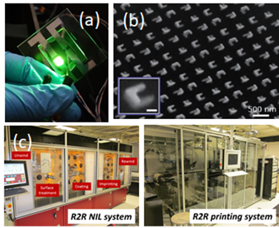
iii) Demonstrate scalable processing methods for materials processing and device fabrication. It is important to develop device platforms that could be amenable to economical processing. With in-house access to roll-to-roll processing, we are well-positioned to carry out small-scale demonstrations of high-throughput, large-area processing to de-risk eventual roll-out of solutions to industrial partners.
Principal Investigators and their primary areas of expertise:
Russel Holmes* Thin film processing; Electrical & optical characterization; Device design (LEDs,photovoltaics, photonic structures), fabrication and testing.
Vivian Ferry Design and fabrication of metamaterials, Plasmonics, Design and synthesis of quantum dots, Photovoltaics and solar concentrators, Optical modeling.
C.Dan Frisbie Processing for printed electronics & devices, Novel patterning methods, Electrical & device characterization.
*Program Leader
Contact: To learn more about the Optoepectronics and Metamaterials Program and IPRIME contact Satish Kumar at kumar030@umn.edu