Review of nanophotonic biosensors in Nature Communications

In a recently published article, a multi-institutional team of scientists including ECE professors Sang-Hyun Oh, Steven Koester, and Tony Low offer a comprehensive review of the potential of van der Waals (vdW) materials in the development of nanophotonic biosensors with advanced capabilities and new applications. The review titled, “Nanophotonic biosensors harnessing van der Waals materials,” is published in Nature Communications, a premier journal that covers the natural sciences. It is the result of scientific collaboration among researchers at the University of Minnesota and other domestic and foreign institutions (names of collaborating institutions and authors included at the end). The article reviews performance metrics of nanophotonic sensors, and how vdW materials can improve their performance, limitations, technological challenges, progress in harnessing these materials, and the road ahead.
VdW materials in nanophotonic biosensors
VdW materials for enhancing SPR biosensors
VdW materials for vibrational spectroscopy
VdW materials as building blocks
Beyond 2D materials
Biosensing tools: the story so far
Biosensing tools that use surface plasmon resonance (SPR) are widely used in the life sciences and medical fields for diagnostic purposes. These photonic biosensors have proven themselves to be highly sensitive detection tools comparable to conventional assays such as enzyme-linked immunosorbent assays (ELISA) or radioimmunoassays. Increasingly used for patient biofluid analysis in clinical settings, SPR-based biosensing eliminates some of the steps involved in sample preparation such as washing and labeling, and have been found to be more sensitive at lower sample volumes as compared to an ELISA assay. The introduction of nanostructures and metasurfaces has extended resonances to frequency ranges from the visible to the near- or mid-infrared (IR), and has given SPR-based sensing tools further advantages including increased sensitivity, multiplexing capability, and miniaturization, all of which are particularly important in biological and diagnostic settings.
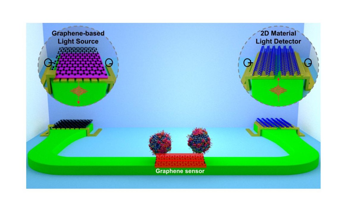
VdW materials in nanophotonic biosensors
While the tightly confined evanescent field of surface plasmon polariton (SPP) waves is confined even further by shaping the gold films into nanoparticles (which gives even greater sensing capability to the extent of a single protein molecule), the introduction of low-dimensional van der Waals (vdW) materials provides additional advantages. The reduced dimensionality of vdW materials such as two-dimensional (2D) graphene can enhance the field confinement further, raising sensitivity and efficiency in comparison to conventional nanophotonic devices. While still a developing sensing technology as compared to ELISA or SPR, two low-dimensional vdW structures, single walled carbon nanotubes (SWNTs), and 2D graphene show a lot of promise. Considering their sensing capabilities that cannot be replicated in metal/dielectric nanophotonic sensors, the reviewers envision these materials going beyond adding greater sensitivity to current assay methods, and initiating new biosensing applications.
Noting that typical performance metrics such as quality factor or resolution might not be applicable to the evaluation of nanophotonic biosensors with different substrate materials, the team have focused on evanescent field decay length as a factor that can characterize the limit of detection (LOD) of disparate biosensors. In practicality, LOD will depend on field decay length, and size of the receptors and analytes, and in the real world, in addition to LOD, factors such as multiplexing capacity, pre-concentration techniques, and signal-enhancing schemes will contribute to the measure of the sensors’ performance.
VdW materials for enhancing SPR biosensors
Gold-film SPR sensors when coated with 2D materials such as graphene have shown improved sensitivity. VdW materials can also be used to protect the surfaces of metals such as copper and silver that are used in SPR biosensing instruments, and their protective properties have been characterized by scientists. However, even as vdW materials are finding a place in SPR sensing applications, they come with disadvantages such as increased complexity, and costs. Increased sensitivity or adsorption offers only marginal gains that are difficult to justify given the significantly higher costs, labor, and complexity of using these materials in SPR sensing applications. According to the review authors, these disadvantages can be offset if scientists seek novel functionalities such as vibrational fingerprinting with spectroscopy, or uses where vdW nanophotonic biosensors are applied in tandem with other sensing modalities such as electrical or electrochemical detection.
VdW materials for vibrational spectroscopy
Graphene and other 2D materials have shown a lot of promise for vibrational spectroscopy because of their electrically tunable doping and ultra confined mid-infrared and terahertz plasmons. IR absorption spectroscopy is an especially powerful tool and can identify the distinct fingerprint created by the vibrational modes of the molecular bonds of samples in solid, liquid, and gas phases. It has many applications within scientific fields and industry. The challenge here is the mismatch between micrometer IR wavelengths and nanometer sized molecules, which means the use of such spectroscopy is limited. However, nanophotonics can overcome the challenge by means of its tightly localized near-fields near resonant optical nanostructures.
The approach is called surface enhanced infrared absorption (SEIRA), and research on low IR signals, an outcome of advances in nanophotonics, has helped expand the potential applications of SEIRA. Although SEIRA has typically used metal-based plasmonic resonators, the entry of novel nanomaterials implies that the shortcomings of metals can now be addressed. Other opportunities for application expansion stem from the unique features of graphene and other 2D vdW materials. Their optoelectronic properties allow external control over plasmonic resonance frequency, and extreme field confinement offers significantly higher sensitivity that can be especially useful for small molecule detection, as well as detection of adsorbed gas molecules.
However low quality graphene can diminish the outcome and the review authors suggest that use in real-world applications will have to wait till the nanofabrication process is refined for the manufacture of high-quality 2D vdW materials that are free of impurities and other defects.
The extreme light confinement in 2D materials, while favorable for increased sensitivity, is accompanied by weak coupling of external light to graphene plasmons, and scientists have used multiple strategies to address the challenge. Strong field confinement also entails that the sample be present on the sensing surface. Although there are several ways by which analytes can be concentrated on the graphene surface, to benefit from them, graphene-based SEIRA devices have to be compatible with in-solution measurements and microfluidics. Although these limitations can be overcome by the use of metal-based SEIRA, graphene and other liquid impermeable vdW materials offer multiple means to avoid water absorption.
VdW materials as building blocks
The review authors indicate that vdW materials can serve as building blocks in the development of compact nanophotonic biosensors. They point to studies that address some of the potential stumbling blocks to the vision, and the demonstrated uses of these materials in the development of biosensors that have increased sensitivity and selectivity. With mid-IR wavelengths indicating expanded detection of biologically relevant molecules, scientists have proposed, developed, and studied waveguide-integrated sensors. These advancements could eventually lead to the elimination of expensive and bulky spectrometers.
Beyond 2D materials: 1D single walled carbon nanotubes
One-dimensional vdW sensor substrates open up even more exciting possibilities: in vivo nanophotonic sensing and bioimaging. The unique properties of single walled carbon nanotubes (SWNTs) have helped develop a technique that can selectively recognize specific molecules. The technique has been used in the detection of a variety of analytes including nitric oxide, proteins, carbohydrates, small molecule drugs and steroids.
Label-free SWNT-based disease detectors have been developed that do away with additional steps after sample collection that are typically associated with traditional methods such as ELISA. The convenience and increased sensitivity of such a biosensor could mean a portable point of care (POC) device that could reduce costs and increase access to timely care. There are several demonstrated examples of these capabilities. The most significant challenge however has to do with biocompatibility of SWNTs; a broad class of materials, the biological response to a formulation has to be evaluated individually. Thus far, scientists have applied SWNTs in animal models with no adverse reactions and successful detection outcomes.
For the authors of the review, the landscape ahead points to multiple opportunities. They envision that scientists will soon be able to harness vdW materials for practical point of care (POC) biosensing applications such as wearable biosensors, and continuous data collection and drug delivery via in vivo sensors. Research in the area could lead to developments that improve functions other than sensing that could eventually advance biosensors. They foresee innovations that will be the outcome of smart combinations of high quality 2D materials, substrates, and device configurations. Taken together, these developments will improve performance, expand application, and increase sensitivity and accuracy of SEIRA-based sensors. The authors predict that work on vdW materials will eventually lead to the “seamless integration of photonics and electronics in the field of biosensing.”
The research team included Sang-Hyun Oh, Tony Low, and Steven J. Koester, University of Minnesota; Hatice Altug, Institute of Bioengineering, École Polytechnique Fédérale de Lausanne (EPFL) in Switzerland; Xiaojia Jin, and Michael S. Strano, Massachusetts Institute of Technology; Aleksander P. Ivanov, and Joshua B. Edel, Imperial College London, UK; and Phaedon Avouris, IBM T.J. Watson Research Center.
The research review was funded by the Minnesota Environment and Natural Resources Trust Fund as recommended by the Legislative-Citizen Commission on Minnesota Resources (LCCMR), Samsung Global Research Outreach (GRO) Program, the European Research Council, the U.S. National Science Foundation, King Abdullah University of Science and Technology, U.K. Biotechnology and Biological Sciences Research Council, U.K. Engineering and Physical Sciences Research Council, the European Research Council, and the Sanford P. Bordeau Chair in Electrical Engineering at the University of Minnesota.