Inside Professor McLeod’s Nano-Imaging Laboratory

Professor Alexander McLeod’s nano-imaging lab creates novel ways to study materials as well as looking for new physics in those materials. Nano-spectroscopy is a technique that attaches conventional optics like lasers and photodetectors to a probe that consists of a tiny, very sharp needle that vibrates 100 thousand times per second. This technique allows physicists to get past the diffraction limit (typically ¼ to ½ the wavelength of the light involved) and “see” materials with nanoscale light at the greatest possible spatial resolution. This technique was first theorized in the late 1920s, but only became technically possible in the 1980s and beyond, with advancements in high-precision nano-positioning and powerful infrared lasers. Recent developments in nanotechnology have motivated physicists to exploit this nano-spectroscopy tool to study materials that will form the basis for future miniaturized electronics.
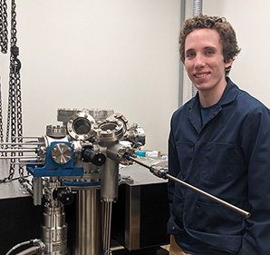
Liam Thompson
In the back room of the lab, third-year student Liam Thompson is building a nano-probe that will operate at low temperatures, as low as the boiling temperature of liquid helium (-450 degrees F), and is preparing a special cryostat that has a small vacuum chamber attached that will house the sample while it is imaged by the nano-probe. The small chamber, the size of a lunchbox, must be pumped out for more than a week to achieve the level of vacuum–100 trillionth of earth’s atmosphere, similar to the surface of the moon–before it can be used for the highest precision measurements. Thompson says that this particular instrument is quite rare, but that Professor McLeod developed one of the first working examples during his Ph.D. thesis. Thompson hopes to push the limits of this technique as well as use the low temperature probe as a research tool for the lab.
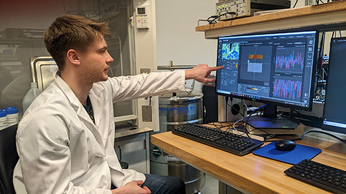
Brayden Lukaskawcez
In another corner of McLeod’s lab, Brayden Lukaskawcez, a first-year student, is running tests on a new type of semiconductor the lab is helping to develop. Generally, new materials are first explored as thin films that are grown on top of a substrate layer that is permanently attached to the material. There are times when a material could be best studied without a substrate. Working with materials scientists in the College of Science and Engineering, the group has added a layer which dissolves in water between the substrate and the growth layer. The semiconductor film can be grown, submerged in water, and the substrate will snap off without harming the material sample. That’s the theory anyway. The reality is a fragile membrane which has shattered. Brayden’s job is to study the shattered membrane to figure out what went wrong and how it can be fixed. After this happy accident, Brayden is also mapping where strain at wrinkles and folds promotes a phase transition into a new crystal structure, endowing the semiconductor with unexpectedly appealing properties. For this, he uses a nano-optical needle attached to a scanning probe microscope on a large table full of lasers and optics. The set up uses two lasers, an infrared guidance laser and an invisible infrared laser that functions as the light source for the probe. Brayden’s work builds on the group’s earlier findings that, even at the small scales of a nanometer-thick membrane, the semiconductor shows a crystal structure just as pristine as its three-dimensional crystal counterparts.
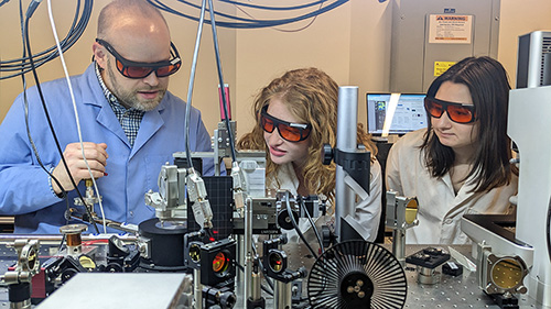
Alexander McLeod, Nitzan Hirshberg and Alyssa Bragg
Following closely along with Brayden’s experiment is third-year graduate student Nitzan Hirshberg. She is scheduled to use the optical nano-probe for her experiments once Brayden finishes his study, but she checks his configuration of the microscope while she prepares her own sample for measurement. Thanks to partnership with the group of Physics Professor Ke Wang, Nitzan plans to study the electrical properties of the smallest crystal realizable in the laboratory, a single atom-thick layer of carbon atoms in a honeycomb lattice called graphene. When two or more monolayers of graphene are stacked together, one atop the other in sequence, the combined structure becomes a “supercrystal”, with electrical properties that vary in space across its surface, but in a periodic pattern that repeats every hundred nanometers or so. Nitzan’s investigations using an optical-probe are one of the few ways to map and study this unique structure, especially since the graphene layers themselves are microscopic in size. It is hoped that close partnership between different research groups in Physics, both preparing unique materials and characterizing them with nano-probes, will accelerate discovery of new material properties that can be engineered down to the nanometer-scale, a “holy grail” ambition that promises future flexible and miniaturized electronics.
Another experiment, recently completed by undergraduate Devon Uram, studies the scattering of light off these nano-probes in minute detail, looking for possible preferred angles that the light might radiate while scattering. New data from this nano-optic study can be compared with detailed simulations of the scattering of light to create more precise and efficient probes for these experiments in the future.