Electronic, Magnetic & Photonic Materials

Functional materials with novel electronic, magnetic, or photonic properties have served as the foundation for innovations in computing, communications, information storage,  and more recently energy conversion and storage. CEMS’ effort in these areas is broad, concerning all aspects of the discovery, processing, characterization, and application of a variety of electronic, magnetic, and photonic materials. The methods employed include first principles theoretical calculations of materials behavior, numerous techniques for the synthesis and preparation of bulk crystals, thin films, and multilayer heterostructures, detailed atomic-level structural and chemical characterization, sophisticated electronic, magnetic, and optical measurements, and application in functional devices. Efforts span the groups of ten faculty members and can be broadly classified as follows:
 

Materials Theory

electronic

Image: Magnetic excitation (spinon) spectrum of spin-1/2 oxyhalide botallackite Cu2(OH)3Br calculated using exact diagonalization, Birol Group

Materials theory and computation are used for a variety of materials systems, giving insight into growth, structure, properties, and devices. Approaches include first-principles theory to explore exotic phases of condensed matter, and discover new materials for superconductors and energy conversion and storage applications, numerical simulations to model crystal growth for electronic and optical applications, and finite-element based simulation of optical and device properties.

Related Faculty and Research Groups:

Electronic and Magnetic Materials & Devices

electronic

Image: Non-Local Spin Valve device, Leighton Group

Research spans a range of materials including both established (e.g., silicon) and emerging (complex oxides, organic, perovskite, quantum dot) semiconductors, as well as metals and insulators. Groups use a broad range of processing methods to prepare both bulk and thin film samples that can be interrogated through a battery of characterization methods or integrated into electronic, magnetic, and optical devices. Numerous micro- and nano-fabrication techniques are used for the latter. Theory is used to explain and predict new applications taking advantage of the correlated and exotic electronic states.

Related Faculty and Research Groups:

Photonics & Optoelectronics

electronic

Image: Light-emitting metamaterial, Ferry group

CEMS researchers are developing a wide variety of materials for photonic and optoelectronic applications. Examples include fundamental study of plasmonics and metamaterials, new methods to pattern large-area nanostructures with unique optical functionality, transparent conductors for power electronics, photovoltaic and photo-detecting devices, and light-emitting devices for next generation displays. Research spans from the development of materials with novel and tunable optical properties, devices with tailored light-matter interactions, and the integration of materials into complete devices with high performance.

Related Faculty and Research Groups:

Sustainability & Energy

electronic

Image: Cross-section of a vapor-processed, metal-halide perovskite solar cell, Holmes Group

Efforts in sustainability and energy are focused on the development of materials and architectures to enable energy harvesting and storage. Of note are CEMS efforts in solar energy conversion with work on a variety of materials platforms (organic, perovskite, pyrite, quantum dot, silicon) as well as integration of these materials into working modules for characterization and qualification.

Related Faculty and Research Groups:

Relevant Collaborative Partners and Core Facilities

Research in electronic, magnetic, and optical research in CEMS is supported by a variety of federal (NSF, DOE, DOD) and industrial partners. Support from NSF includes participation of several PIs in the Materials Research Science and Engineering Center (MRSEC). In addition, several PIs participate in the UMN Industrial Partnership for Research in Interfacial and Materials Engineering (IPRIME) via the Coating Process Fundamentals and Optoelectronics and Metamaterials programs, as well as the DOE-funded Center for Quantum Materials Researchers also make use of the UMN Characterization Facility (CharFac) and the microelectronics processing and nanofabrication capabilities in the Minnesota Nano Center (MNC).

Major Funding Sources

Publications and Patents

Expand all

Room temperature valence transition in a strain-tuned perovskite oxide

electronic

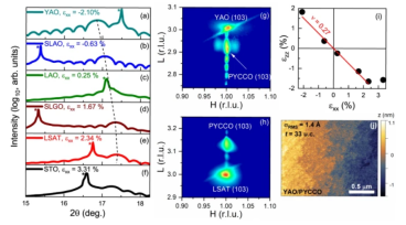
Cobalt oxides have long been understood to display intriguing phenomena known as spin-state crossovers, where the cobalt ion spin changes vs. temperature, pressure, etc. A very different situation was recently uncovered in praseodymium-containing cobalt oxides, where a first-order coupled spin-state/structural/metal-insulator transition occurs, driven by Read More...

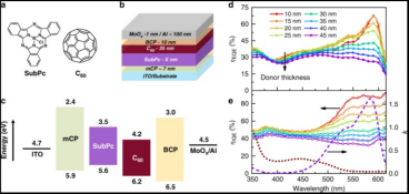
Polarization-Induced Exciton–Polaron Quenching in Organic Light-Emitting Devices and Its Control by Dipolar Doping

pub

Many electron transport layer (ETL) materials employed in organic light-emitting devices (OLEDs) show a preferred orientation of the molecular permanent dipole moments. This phenomenon is known as spontaneous orientation polarization (SOP) and results in the formation of bound polarization charge. In an OLED, this leads to the accumulation of Read More...

Imaging Nanometer Phonon Softening at Crystal Surface Steps with 4D Ultrafast Electron Microscopy

pub

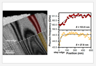
Step edges are an important and prevalent topological feature that influence catalytic, electronic, vibrational, and structural properties arising from modulation of atomic-scale force fields due to edge-atom relaxation. Direct probing of ultrafast atomic-to-nanoscale lattice dynamics at individual steps poses a particularly significant challenge owing to Read More...

Intrinsic measurements of exciton transport in photovoltaic cells

pub

Organic photovoltaic cells are particularly sensitive to exciton harvesting and are thus, a useful platform for the characterization of exciton diffusion. While device photocurrent spectroscopy can be used to extract the exciton diffusion length, this method is frequently limited by unknown interfacial recombination losses. We resolve this limitation and demonstrate a general, device-based photocurrent-ratio measurement to Read More...

Optical properties of electrochemically gated La1-xSrxCoO3-d as a topotactic phase-change material

pub

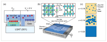
Materials with tunable infrared refractive index changes have enabled active metasurfaces for novel control of optical circuits, thermal radiation, and more. Ion-gel-gated epitaxial films of the perovskite cobaltite La1−xSrxCoO3−δ (LSCO) with 0.00 ≤ x ≤ 0.70 offer a new route to significant, voltage-tuned, nonvolatile refractive index modulation for infrared active metasurfaces, shown here through Read More...

Optical approaches for passive thermal management in c-Si photovoltaic modules

pub

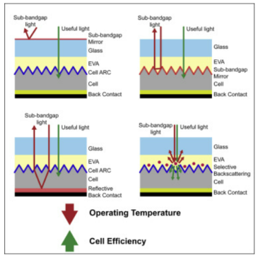
Elevated operating temperatures of solar cells encapsulated in modules lead to reduced efficiency and module lifetime. Here, we provide a comprehensive overview of the challenges and opportunities for passive optical thermal management of PV modules based on the rejection of sub-band-gap light by idealized reflectors and scatterers applied at different interfaces within crystalline Si modules and discuss Read More...

Room-temperature high spin–orbit torque due to quantum confinement in sputtered BixSe(1–x) films

pub

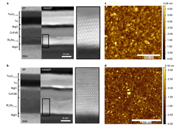
The spin–orbit torque (SOT) that arises from materials with large spin–orbit coupling promises a path for ultralow power and fast magnetic-based storage and computational devices. We investigated the SOT from magnetron-sputtered BixSe(1–x) thin films in BixSe(1–x)/Co20Fe60B20 heterostructures by using d.c. planar Hall and spin-torque ferromagnetic resonance (ST-FMR) methods. Remarkably, the spin torque efficiency (θS) was determined to be as large as Read More...