Materials Processing
Materials processing transforms raw materials into useful forms, such as coatings, films, fibers and complex shapes, with well-defined structure and properties. It plays a central role in the large-scale manufacturing of a wide variety of products for electrical, mechanical, thermal, biomedical and optical applications. Materials processing is inherently interdisciplinary and forms a natural bridge between basic and applied science and engineering. In some cases, research in CEMS develops and applies processing science to enable the production of new materials and microstructures predicted to have unique or improved properties. In other cases, processing-related research focuses on understanding the fundamental phenomena to enable industrial scale-up of manufacturing processes with improved efficiency and product quality.
Coating & Printing Processes
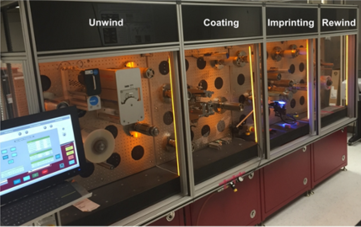
Coatings, films and printed patterns are everywhere! They are commonly made by depositing liquids, such as polymer solutions and ceramic particle suspensions, onto substrates, followed by solidification through drying, sintering or curing to develop the required functional properties, such as wear resistance and antireflection. Liquid applied coating and printing processes are frequently carried out via fast and economical roll-to-roll (R2R) processes. In CEMS, we have a long history of fundamental research on coating and printing processes, and we have recently applied our expertise to the challenge of developing R2R printed electronics.
Related Faculty and Research Groups:
Polymer Processing
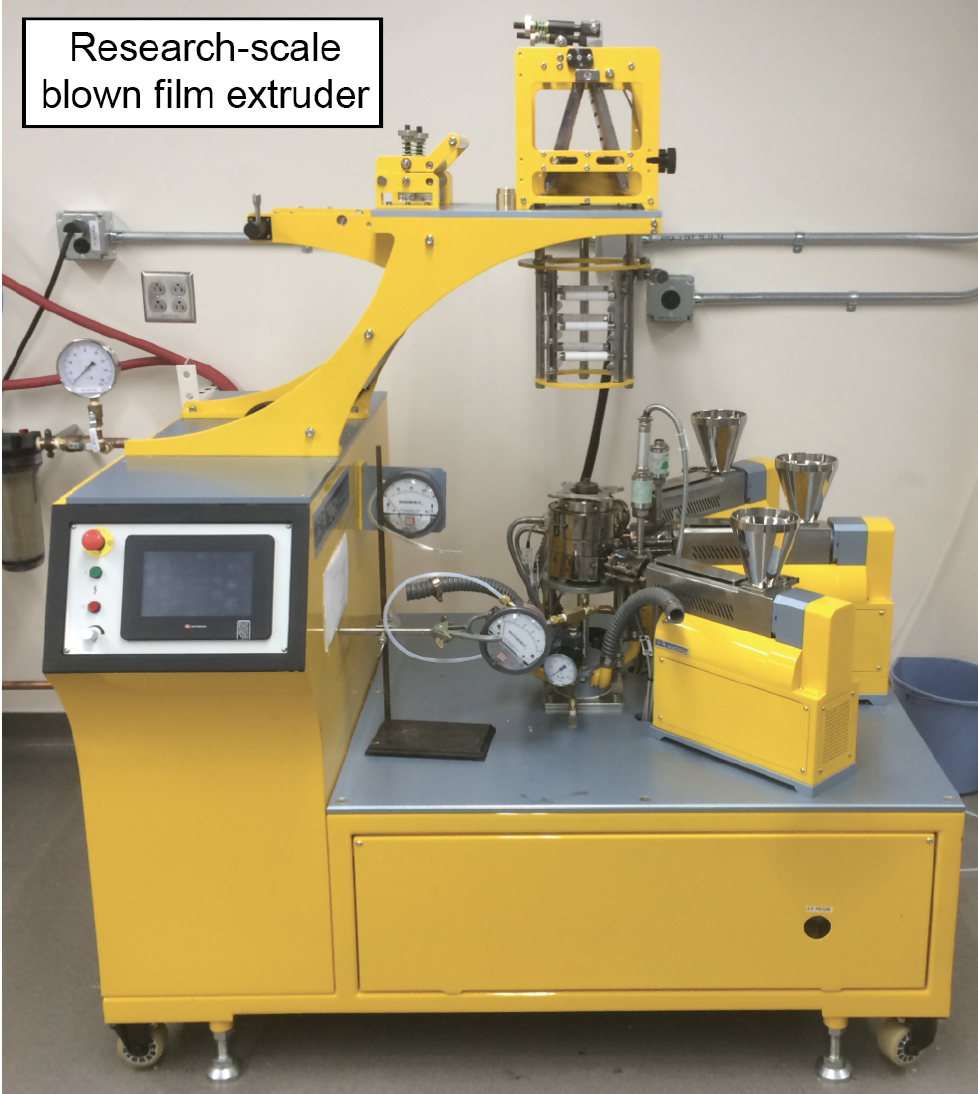
Polymers are processed into complex shapes with well-designed structures and properties. The exploration and synthesis of new polymers, such as nanostructured block polymers and tunable elastomers, is closely coupled to the engineering of processing routes, such as injection molding and blown film extrusion, that are designed to further develop properties and functionality of polymer materials. The section on Polymer Science and Engineering provides more information.
Related Faculty and Research Groups:
- Microstructured Polymers Program of IPRIME
- Frank Bates - Bates Research Group
- Michelle Calabrese - Calabrese Research Group
- Chris Ellison - Ellison Research Group
- Lynn Walker
Vapor Phase Thin Film Deposition
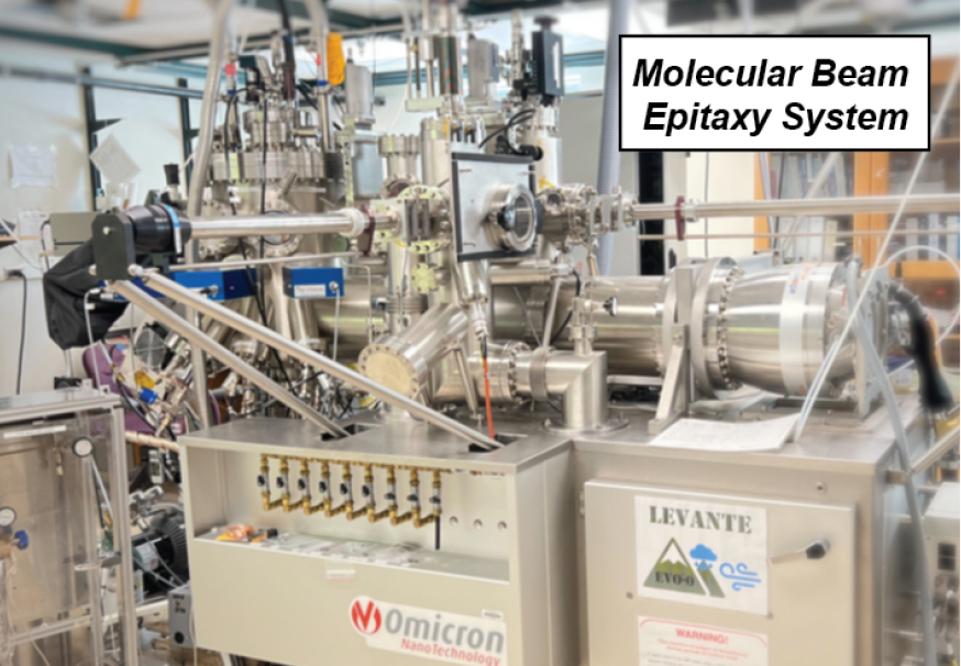
Many functional materials derive their unique properties through careful control of composition and crystal structure, and devices require precise heterostructure architectures only achievable using specialized processes. Research in this area develops and applies a variety of techniques such as molecular beam epitaxy (MBE), sputtering, thermal and electron beam evaporation, atomic layer deposition ALD) and physical and chemical vapor deposition (PVD, CVD) to produce thin films with engineered morphology from novel materials. Nanofabrication and lithographic techniques can then be used to produce devices. See our research overview on Electronic, Magnetic & Photonic Materials to learn more about research in CEMS related to the application of films produced using these techniques.
Related Faculty and Research Groups:
Additive Manufacturing

Additive manufacturing is revolutionizing the field of materials processing by allowing fabrication of metals, ceramics and polymers with complex and customizable shapes and little to no waste. Additive processes include those developed to produce 3D shapes, such as fused filament fabrication of polymers and selective laser melting of metals as well as those that create 2D patterns additively, such as ink jet printing.
Related Faculty and Research Groups:
Bulk Metal & Ceramic Processing
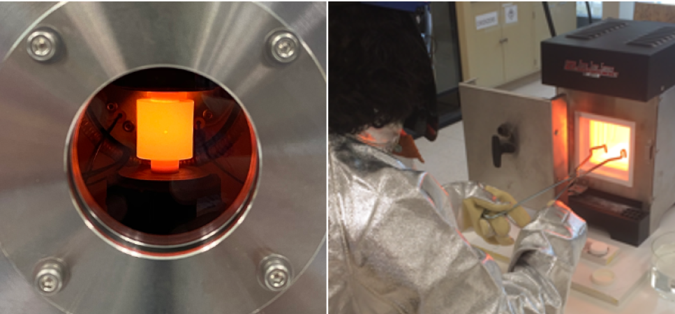
A variety of powder, melt, and solid deformation approaches are used to process bulk metal and ceramic materials to achieve the desired composition and microstructure, whether it be understanding and controlling the growth of large single crystals or achieving a controlled polycrystalline microstructures. Common techniques include vacuum arc melting, pressureless sintering, hot pressing, current-assisted densification, and rolling. These methods are used routinely to synthesize novel compositions and to elucidate processing-structure-property relationships.
Related Faculty and Research Groups:
Relevant Collaborative Partners and Core Facilities
Processing-related research in CEMS benefits from close collaborations with industrial partners, such as those supported in the Coating Process Fundamentals, Microstructured Polymers, and Optoelectronics and Metamaterials research groups within the Industrial Partnership for Research in Interfacial and Materials Engineering (IPRIME) and through research supported by the NSF-funded Materials Research Science and Engineering Center (MRSEC). This research also makes use of shared facilities for processing and characterization including the UMN Characterization Facility (CharFac), the Polymer Characterization and Processing Facility, and cleanroom and microelectronics processing capability in the Minnesota Nano Center (MNC).
Selected Publications
+
Process Engineered Spontaneous Orientation Polarization in Organic Light-Emitting Devices
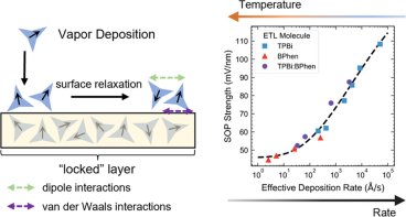
Polar molecules with appreciable permanent dipole moments (PDMs) are widely used as the electron transport layer (ETL) in organic light-emitting devices (OLEDs). When the PDMs spontaneously align, a macroscopic polarization field can be observed, a phenomenon known as spontaneous orientation polarization (SOP). The Read More...
Related Faculty: Russell Holmes
+
Solution-based, additive fabrication of flush metal conductors in plastic substrates by printing and plating in two-level capillary channels
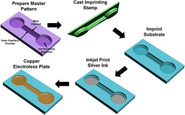
A strategy to control the structure of electroless copper deposition in confined features was developed for applications in printed electronic devices and interconnects. This work builds on and refines a previous process of additively manufacturing metal conductors using a combined imprint, print, and plate strategy. A two-level Read More...
Related Faculty: Lorraine Francis, Dan Frisbie
+
Structure-Property Relationships and Mobility Optimization in Sputtered La-doped BaSnO3 Films: Toward 100 cm2V-1s-1 Mobility
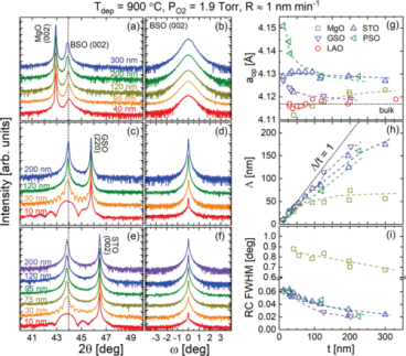
The wide band gap semiconducting perovskite BaSnO3 is of high current interest due to outstanding room temperature mobility at high electron density, fueled by potential applications in oxide, transparent, and power electronics. Due in part to a lack of lattice-matched substrates, BaSnO3 thin films suffer from Read More...
Related Faculty: Bharat Jalan, Chris Leighton, Andre Mkhoyan
+
Gas Nitriding Behavior of Refractory Metals and Implications for Multi-Principal Element Alloy Design
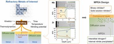
Multi-principal element alloys (MPEAs) comprise a large, flexible compositional space that enables tuning of their chemistry, structure, and properties. To facilitate the development of nitriding-based surface-enhancement strategies that harness a broad compositional space, this study examined Read More...
Related Faculty: Nate Mara, David Poerschke
+
Photocrosslinkable Polymeric Bicontinuous Microemulsions
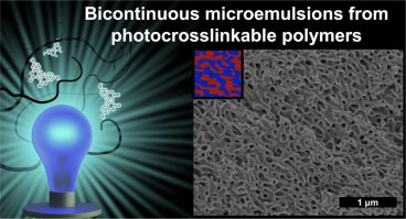
We present an approach to photocrosslink bicontinuous microemulsions derived from ternary blends of poly(methoxyethyl acrylate) (PM, Mn = 4200 g/mol), poly(hexyl methacrylate-co-coumarin methacrylate) (PHC, Mn = 6800 g/mol), and PM-b-PHC diblock polymer (Mn = 19,400 g/mol) in a phase-selective manner, enabling structural characterization at an Read More...
Related Faculty: Frank Bates, Tim Lodge
+
Engineering Metal Oxidation using Epitaxial Strain
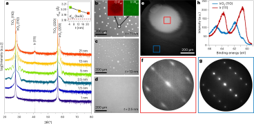
The oxides of platinum group metals are promising for future electronics and spintronics due to the delicate interplay of spin-orbit coupling and electron correlation energies. However, their synthesis as thin films remains challenging due to their low vapour pressures and low oxidation potentials. Here we show Read More...
Related Faculty: Bharat Jalan, Andre Mkhoyan